NEW LAYOUTS HAVE BEEN IMPLEMENTED !!!!
In my dreams I had a vision of building a directable loop-antenna with reasonable physical dimensions, together with a low distorsion and low noise RF-amplifier. Then I stumbled over a paper written by Chris Trask in 2010 with a RF-amplifier suitable for a loop-antenna: ”A High Dynamic Range Amplifier for Wideband Active Loop Antennas”.
This was exactly what I had dreamed of, but then it was the job to build it! During at least 5 years I have from time to time been thinking of how to make the best solutions for the layout. And now I have come to the end of this thinking. It has to be built! The components for the amplifier have been bought from Mouser and via Ebay. Then my health paused it all. What to do?
If I don’t build it, maybe some other DX-er want to do so?! Thats why I publish my thoughts without showing a ”real life version”.
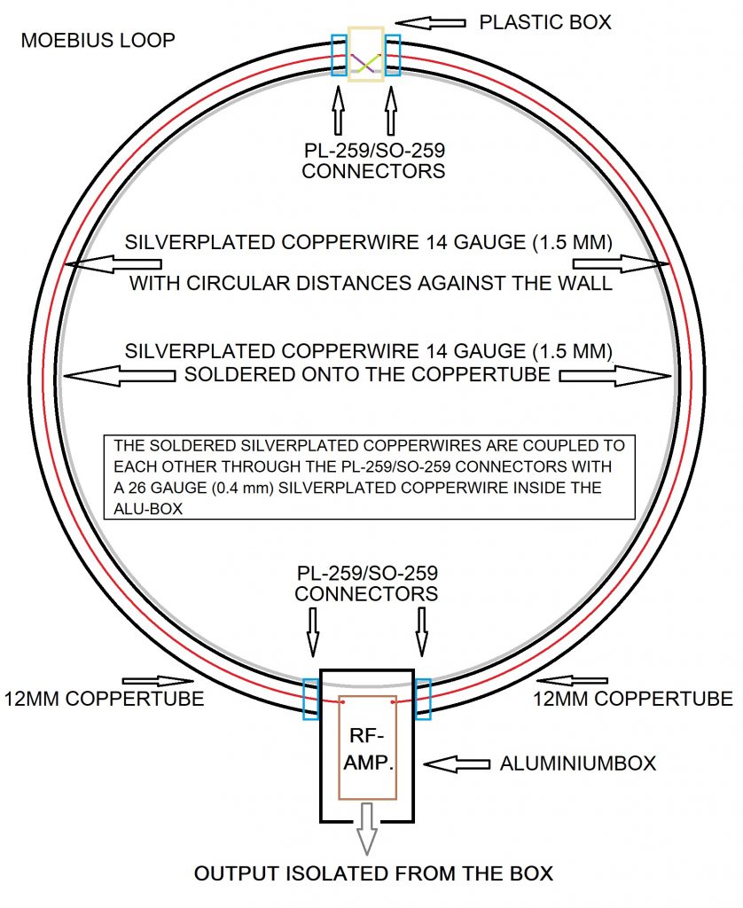
There are two versions of the antenna, the shielded loop and the Moebius loop. My plan was to build it with 1 m diameter, the coppertubes has already been recovered and bent into the right shape. Here comes the suggested layouts for the constructions:
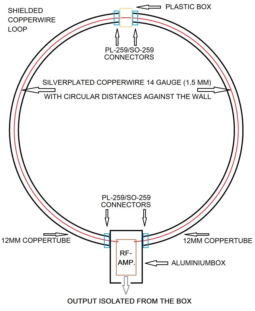
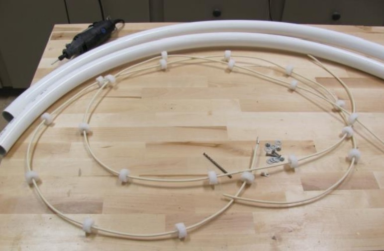
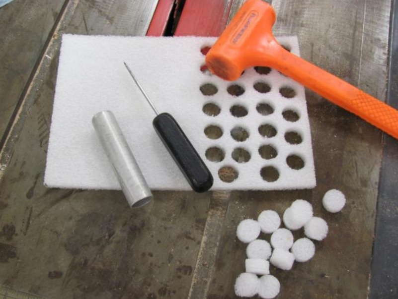
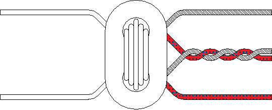
The inner silverplated copperwire is hold in the middle of the coppertube with polyfoam discs. See photos below (from Medium Wave News 62/02 by Everett Sharp N4CY (everettsharp@aol.com)). By doing this homebrew coax the capacitance of the antenna gets lower.
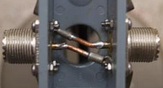
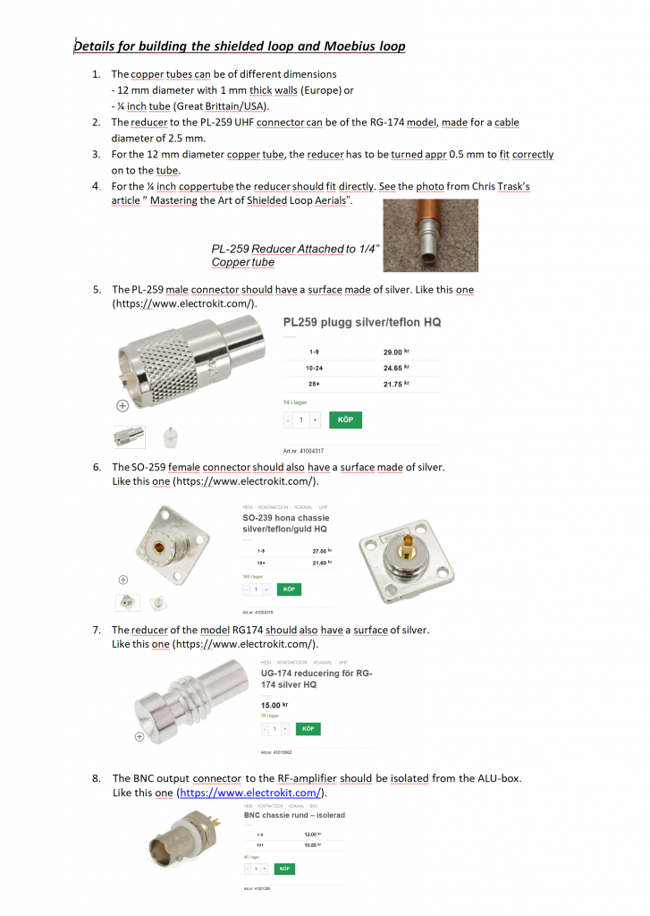
The top box of these loops has to be of non-shielding material. And the cross-connection on the Moebius loop can be done as in this photo from Chris Trask’s paper “Mastering the Art of Shielded Loop Aerials” from 2010.
The outer end of the inner silverplated copperwire has to be shielded from getting in contact to the reducer when soldered to the tip of the PL-259 UHF male connector. This can be done with shrinktube.
And there are certain details that I think can be of interest:
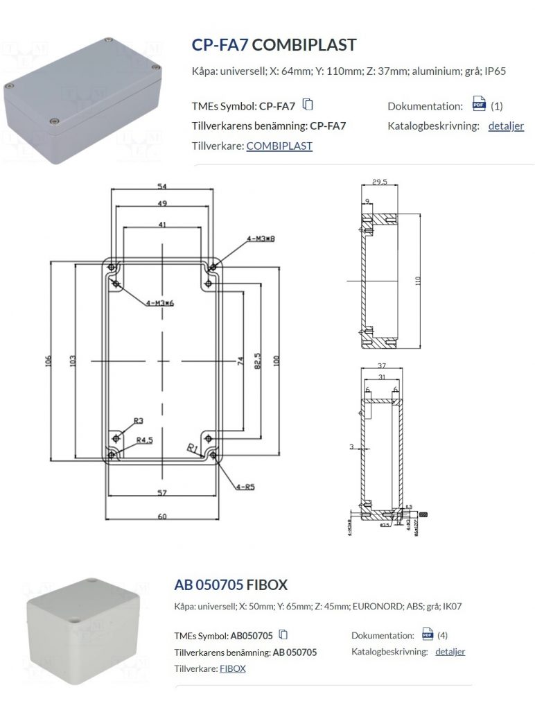
The holder of the loop (the sides of the ALU-box) needs to be rather thick to withstand the stress that wind and torsion gives to the antenna-construction. I found suitable boxes for the construction at TME (https://www.tme.eu/), the ALU-box with 3 mm wall thickness and a plastic box for the top of the antenna:
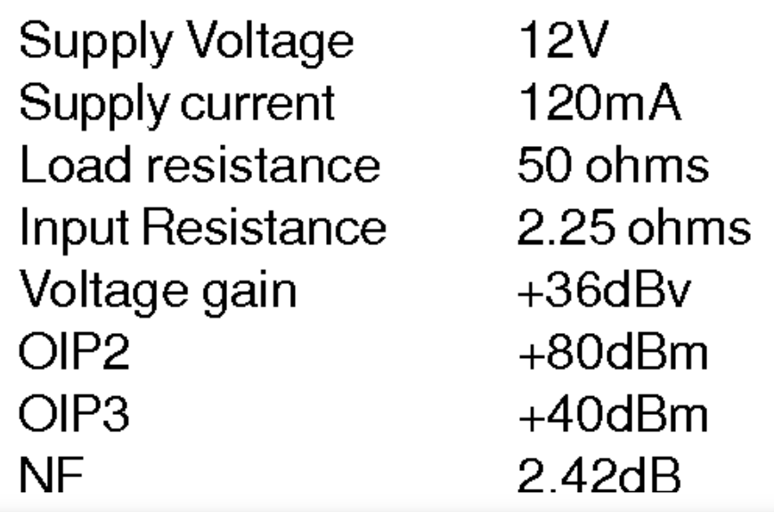
And lastly: A High Dynamic Range Amplifier for Wideband Active Loop Antennas
When I now was to design this text I can’t find the PDF online any more?! The only parts online of the paper on this RF-amplifier, written by Chris Trask, are the schematics and some instructions and photos of transformers. I have therefore here inserted some text describing details when making the transformers and how they are to be connected to the curcuit.
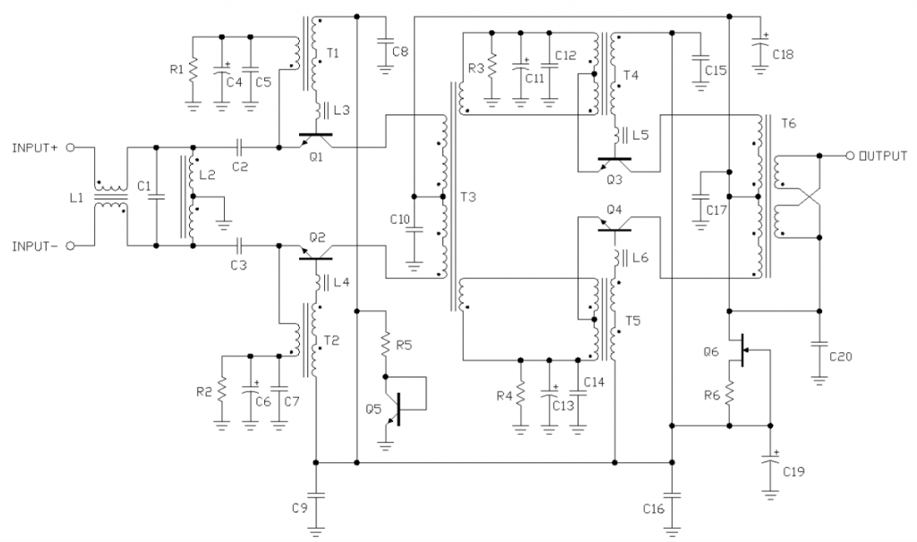
And don’t forget the ferrit beads on the transistor base on Q1-4!!!
There are 6 transformers in this curcuit.
A good idea is to protect the curciut from shortcuts between the transformer cores to the stripes on the PCB. Use doublesided tape under the cores!
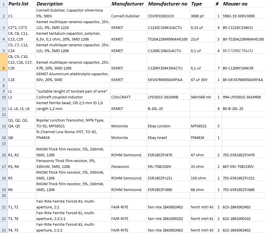
The T1 and T2 are the transformers in the input stage. They are made with 4 turns trifilar 32 AWG (0.2 mm) wound on a FairRite 2843002402 binocular core made of material 43.
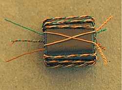
It’s very convinient to mark the wires in different colours. I use to draw the wires against a protective surface under the tip of a pen with permanent colour and let them dry for at least 15 minutes before using them.
The two neutral wires to the left, in the figure above, are the primary winding. At the right end we see the wires for the secondary winding, with the two joined center wires. Keep in mind to connect the transformers in the right way to the curcuit.
For the T1 the connections are as follows: the lower right (red), in the figure above, connects to the transistor base and the upper left (neutral) to the transistor emitter. The upper right (black/gray) is connected to C8, and the lower left (neutral) is connected to R1, C4, C5.
For the T2 the connections are as follows: the upper right (black/gray), in the figure above, connects to the transistor base, and the lower left (neutral) to the transistor emitter. The lower right (red) is connected to C9, and the upper left (neutral) is connected to R2, C6, C7.
The transformers T4 and T5 are made with 4 turnes of a twisted bifilar wire AWG 32 (0.2 mm), wound on the outside of each hole of a FairRite 2843002402 binocular core.
For the T4 the connections are as follows: the lower right (black/gray), in the figure above, connects to the transistor base on Q3 and the joined center wires (red), in the right end, connects to the transistor emitter on Q3. The upper right (black/gray) connects to C15.
For the T5 the connections are as follows: the upper right (black/gray), in the figure above, connects to the transistor base on Q4 and the joined center wires (red), in the right end, connects to the transistor emitter on Q4. The lower right (black/gray) connects to C16/C19.
Both red wires on the left side, in the figure above, are incoming from T3. Where on the T4 the lower left (red) connects to the “cold end” (to R3, C11, C12), and the upper left (red) connects to the signal wire from T3.
On the T5 the upper left (red) connects to the “cold end” (to R4, C13, C14), and the lower left (red) connects to the signal wire from T3.
The joined wires on the left side on both the T4 and T5 (black/gray) are left soldered together therebye forming the secondary winding.
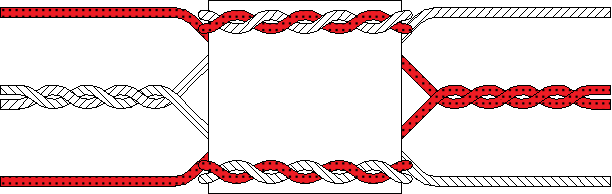
The T3 and T6 are a bit similar in construction as the T4 and T5, they are all made with wires wound on the outside of the cores. But the big difference is that the T3 and T6 are made with a bigger sized Fair-Rite 2861000102 binocular core made of material 61 and with trifilar wire.
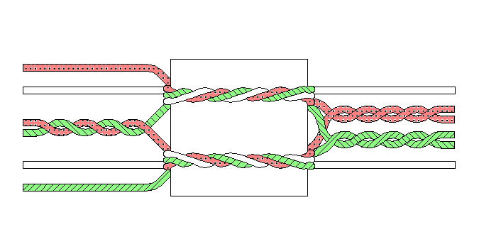
The T3 is made with 6 turnes of AWG 30 (0.25 mm) twisted trifilar wire wound along the outside of each core holes. Beginning from the bottom surface of the core hole up to the top surface and down on the outside and so on. At the right end of the core, see the figure above, the red wires are joined together, and then the green wires are joined together.
At the same end of the core, the two neutral wires are the terminals of the signal wires from T3. The upper right (neutral) wire, in the figure above, is connected to the transformer T4, and the lower right (neutral) wire, in the figure above, is connected to the transformer T5.
Of the incoming wires on the left side of the core, in the figure above, the upper (red) wire is connected to the Q1 collector and the lower (green) wire is connected to the Q2 collector.
The joined red and green wire on the left side of the core, are the centertap of the T3 primary winding. They are soldered to the “hookedlike” stripe on the PCB.
The remaining neutral wires, on the left side of the core, are connected on the left side of the core via the stripes on the PCB: the upper left wire, in the figure above, is connected to the “cold end” of T4 and R3, C11, C12. The lower left wire, in the figure above, is connected to the “cold end” of T5 and R4, C13, C14.
The T6 is made almost in the same way as the T3. The only difference when making it, is that the neutral wires on the left side of the core, in the figure above, are bent crosswise under the core and joined with the neutral wires on the right side of the core. See the photo below from the paper written by Chris Trask.
Connecting the T6 is done as follows: The crosswise joined neutral wires are now on the right side of the core. The upper right joined wires are soldered to the point on the PCB with contact to the positive side of the supplyvoltage and the lower right joined wires are soldered to the point on the PCB with contact to the incoming from the BNC connector.
The upper left red wire, in the figure above, connects to the collector of Q3. The lower left green wire, in the figure above, connects to the collector of Q4. The centerwire on the left side of the core is connected to the solderingpoint wih contact to C10.
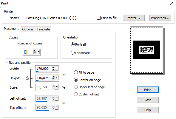
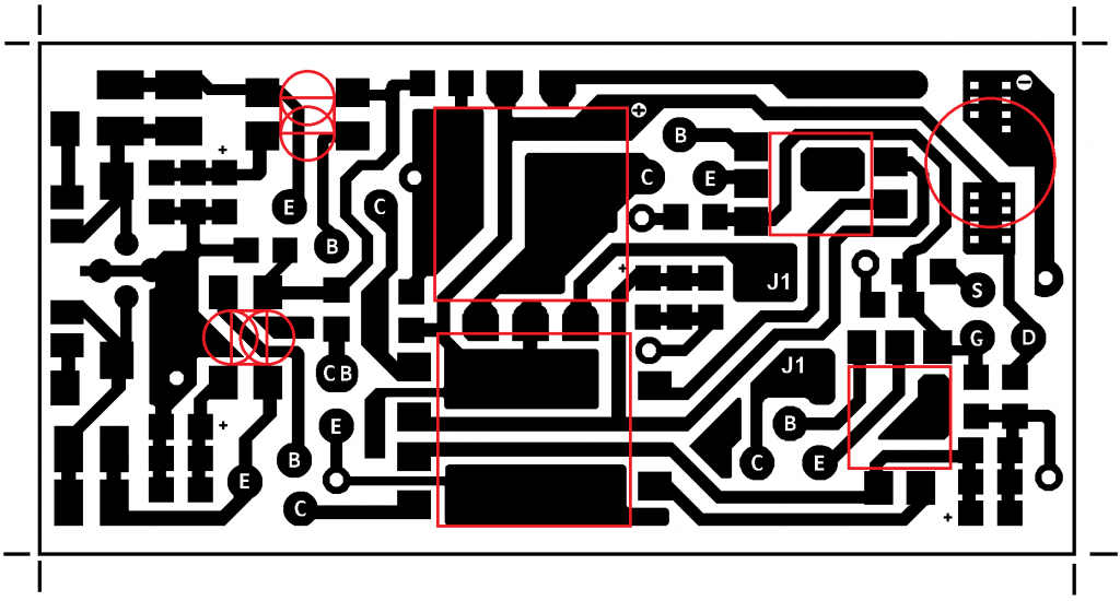
The layouts looks like this:
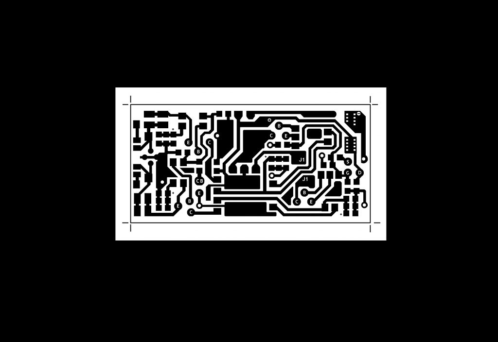
Print it with these settings (my printing is done with Corel PaintShop Pro):
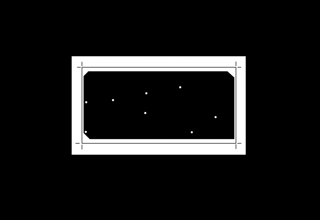
Here comes the ground plane
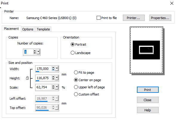
With the print settings like these (my printing is done with Corel PaintShop Pro):
And of course here is where the components are to be set:
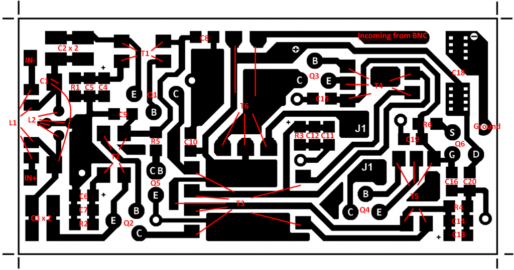
I have also made a layout showing how larger components are placed.
I have found it easier to make double sided PCBs from two one sided etched laminates. I found a 0.8 mm laminate at Electrokit. You just glue them together after adjusting the laminates to fit the predrilled holes. Then solder the ground connections between the layers before mounting the rest of the components.